
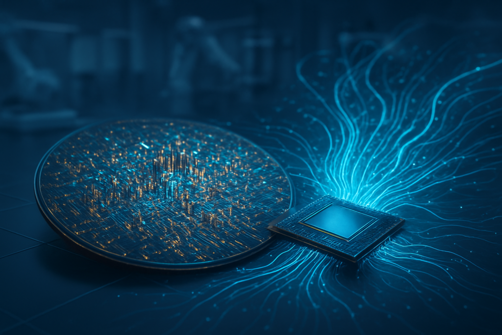
As the global semiconductor race enters the "Angstrom Era," Taiwan Semiconductor Manufacturing Company (NYSE: TSM) has achieved a critical breakthrough that solidifies its dominance over the next generation of artificial intelligence and mobile silicon. Industry reports as of January 23, 2026, confirm that TSMC’s Baoshan Fab 20 has successfully stabilized yield rates for its 2nm (N2) process technology at a remarkable 70% to 80%. This milestone arrives just in time to support the mass production of the Apple (NASDAQ: AAPL) A20 chip, the powerhouse expected to drive the upcoming iPhone 18 Pro series.
The achievement marks a pivotal moment for the industry, as TSMC successfully transitions from the long-standing FinFET transistor architecture to the more complex Nanosheet Gate-All-Around (GAAFET) design. While the technical triumph is significant, it comes with a staggering price tag: 2nm wafers are now commanding roughly $30,000 each. This "silicon cost crisis" is reshaping the economics of high-end electronics, even as TSMC races to scale its production capacity to a target of 100,000 wafers per month by late 2026.
The Technical Leap: Nanosheets and SRAM Success
The shift to the N2 node is more than a simple iterative shrink; it represents the most significant architectural overhaul in semiconductor manufacturing in over a decade. By utilizing Nanosheet GAAFET, TSMC has managed to wrap the gate around all four sides of the channel, providing superior control over current flow and significantly reducing power leakage. Technical specifications for the N2 process indicate a 15% performance boost at the same power level, or a 25–30% reduction in power consumption compared to the previous 3nm (N3E) generation. These gains are essential for the next wave of "AI PCs" and mobile devices that require immense local processing power for generative AI tasks without obliterating battery life.
Internal data from the Baoshan "mother fab" indicates that logic test chip yields have stabilized in the 70-80% range, a figure that has stunned industry analysts. Perhaps even more impressive is the yield for SRAM (Static Random-Access Memory), which is reportedly exceeding 90%. In an era where AI accelerators and high-performance CPUs are increasingly memory-constrained, high SRAM yields are critical for integrating the massive on-chip caches required to feed hungry neural processing units. Experts in the research community have noted that TSMC’s ability to hit these yield targets so early in the HVM (High-Volume Manufacturing) cycle stands in stark contrast to the difficulties faced by competitors attempting similar transitions.
The Apple Factor and the $30,000 Wafer Cost
As has been the case for the last decade, Apple remains the primary catalyst for TSMC’s leading-edge nodes. The Cupertino-based giant has reportedly secured over 50% of the initial 2nm capacity for its A20 and A20 Pro chips. However, the A20 is not just a die-shrink; it is expected to be the first consumer chip to utilize Wafer-Level Multi-Chip Module (WMCM) packaging. This advanced technique allows RAM to be integrated directly alongside the silicon die, dramatically increasing interconnect speeds. This synergy of 2nm transistors and advanced packaging is what Apple hopes will keep it ahead of the pack in the burgeoning "Mobile AI" wars.
The financial implications of this technology are, however, daunting. At $30,000 per wafer, the 2nm node is roughly 50% more expensive than the 3nm process it replaces. For a company like Apple, this translates to an estimated cost of $280 per A20 processor—nearly double the cost of the chips found in previous generations. This price pressure is likely to ripple through the entire tech ecosystem, forcing competitors like Nvidia (NASDAQ: NVDA) and Advanced Micro Devices (NASDAQ: AMD) to choose between thinning margins or passing the costs on to enterprises. Meanwhile, the yield gap has left Samsung (KRX: 005930) and Intel (NASDAQ: INTC) in a difficult position; reports suggest Samsung’s 2nm yields are still hovering near 40%, while Intel’s 18A node is struggling at 55%, further concentrating market power in Taiwan.
The Broader AI Landscape: Why 2nm Matters
The stabilization of 2nm yields at Fab 20 is not merely a corporate win; it is a critical infrastructure update for the global AI landscape. As large language models (LLMs) move from massive data centers to "on-device" execution, the efficiency of the silicon becomes the primary bottleneck. The 30% power reduction offered by the N2 process is the "holy grail" for hardware manufacturers looking to run complex AI agents natively on smartphones and laptops. Without the efficiency of the 2nm node, the heat and power requirements of next-generation AI would likely remain tethered to the cloud, limiting privacy and increasing latency.
Furthermore, the geopolitical significance of the Baoshan and Kaohsiung facilities cannot be overstated. With TSMC targeting a massive scale-up to 100,000 wafers per month by the end of 2026, Taiwan remains the undisputed center of gravity for the world’s most advanced computing power. This concentration of technology has led to renewed discussions regarding "Silicon Shield" diplomacy, as the world’s most valuable companies—from Apple to Nvidia—are now fundamentally dependent on the output of a few square miles in Hsinchu and Kaohsiung. The successful ramp of 2nm essentially resets the clock on the competition, giving TSMC a multi-year lead in the race to 1.4nm and beyond.
Future Horizons: From 2nm to the A14 Node
Looking ahead, the roadmap for TSMC involves a rapid diversification of the 2nm family. Following the initial N2 launch, the company is already preparing "N2P" (enhanced performance) and "N2X" (high-performance computing) variants for 2027. More importantly, the lessons learned at Baoshan are already being applied to the development of the 1.4nm (A14) node. TSMC’s strategy of integrating 2nm manufacturing with high-speed packaging, as seen in the recent media tour of the Chiayi AP7 facility, suggests that the future of silicon isn't just about smaller transistors, but about how those transistors are stitched together.
The immediate challenge for TSMC and its partners will be managing the sheer scale of the 100,000-wafer-per-month goal. Reaching this capacity by late 2026 will require a flawless execution of the Kaohsiung Fab 22 expansion. Analysts predict that if TSMC maintains its 80% yield rate during this scale-up, it will effectively corner the market for high-end AI silicon for the remainder of the decade. The industry will also be watching closely to see if the high costs of the 2nm node lead to a "two-tier" smartphone market, where only the "Ultra" or "Pro" models can afford the latest silicon, while base models are relegated to older, more affordable nodes.
Final Assessment: A New Benchmark in Semiconductor History
TSMC’s progress in early 2026 confirms its status as the linchpin of the modern technology world. By stabilizing 2nm yields at 70-80% ahead of the Apple A20 launch, the company has cleared the highest technical hurdle in the history of the semiconductor industry. The transition to GAAFET architecture was fraught with risk, yet TSMC has emerged with a process that is both viable and highly efficient. While the $30,000 per wafer cost remains a significant barrier to entry, it is a price that the market’s leaders seem more than willing to pay for a competitive edge in AI.
The coming months will be defined by the race to 100,000 wafers. As Fab 20 and Fab 22 continue their ramp, the focus will shift from "can it be made?" to "who can afford it?" For now, TSMC has silenced the doubters and set a new benchmark for what is possible at the edge of physics. With the A20 chip entering mass production and yields holding steady, the 2nm era has officially arrived, promising a future of unprecedented computational power—at an unprecedented price.
This content is intended for informational purposes only and represents analysis of current AI developments.
TokenRing AI delivers enterprise-grade solutions for multi-agent AI workflow orchestration, AI-powered development tools, and seamless remote collaboration platforms.
For more information, visit https://www.tokenring.ai/.